In the ever-evolving world of electronics and technology, the demand for semiconductor chips has skyrocketed. These tiny wonders power everything from smartphones and laptops to advanced medical devices and self-driving cars. However, the manufacturing of these chips comes with a significant environmental cost. Enter Wafer Reclaiming, a process that aims to minimize waste and maximize the utilization of valuable resources.
Understanding Semiconductor Wafers:
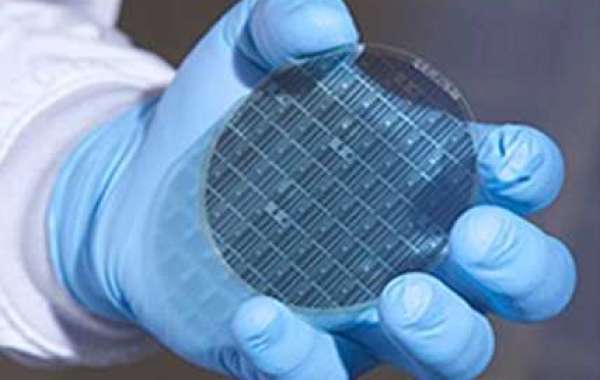
Before delving into the intricacies of wafers and reclaiming, let's first understand what semiconductor wafers are and their role in chip manufacturing. Semiconductor wafers are thin slices of crystalline silicon that serve as the foundation for creating integrated circuits. These wafers undergo multiple complex processes, including deposition, etching, and doping, to form the intricate patterns and structures that enable electronic devices to function.
The Challenge of Waste Generation:
The production of semiconductor wafers is a highly precise and intricate process. Unfortunately, it also generates a significant amount of waste. During manufacturing, defects, impurities, and process variations can render some wafers unsuitable for use in the final product. Additionally, in the fabrication process, wafer edges are often trimmed, resulting in leftover silicon that goes to waste.
The Promise of Wafer Reclaiming:
Wafer reclaiming, also known as wafer recycling or wafer refurbishment, offers a promising solution to tackle the waste generated during semiconductor manufacturing. This process involves the restoration and reuse of rejected or discarded wafers, making them suitable for further fabrication. Wafers and reclaiming not only reduce waste but also minimize the consumption of raw materials, energy, and water in the production of new wafers.
The Wafer Reclaiming Process:
- Wafer Sorting
The first step in wafers and reclaiming is the sorting of discarded wafers. These wafers are carefully inspected and classified based on their defects, such as scratches, contamination, or excessive thinning. Sorting ensures that only wafers with reclaimable potential move forward in the process, while severely damaged or irreparable wafers are appropriately disposed of.
- Wafer Stripping
Once the reclaimable wafers are selected, the next stage is wafer stripping. In this step, the existing layers and circuit patterns on the wafer are removed using chemical processes. The stripping process cleans the surface of the wafer, preparing it for subsequent layers or deposition.
- Polishing and Planarization
After the stripping process, the wafer undergoes polishing and planarization to remove any remaining imperfections or surface irregularities. Polishing smoothens the wafer surface, ensuring a uniform and defect-free substrate for subsequent processes.
- Cleaning and Surface Preparation
The wafer is thoroughly cleaned and rinsed to remove any residual particles, chemicals, or contaminants. This step is crucial to maintain the purity of the wafer surface and ensure the quality of the subsequent fabrication processes.
- Deposition and Doping
Once the reclaimed wafer is cleaned and prepared, it is ready for deposition and doping processes. Thin layers of various materials are deposited on the wafer surface, creating the desired circuit patterns and structures. Doping involves introducing impurities into specific regions of the wafer to modify its electrical properties.
- Quality Control and Testing
After the deposition and doping processes, the reclaimed wafers undergo rigorous quality control measures. They are tested for electrical performance, structural integrity, and reliability. Any wafers that do not meet the required specifications are sent back for further reclamation or proper disposal.
- Integration into the Manufacturing Flow
Once the reclaimed wafers pass the quality control tests, they are integrated back into the manufacturing flow. They go through subsequent processes, such as lithography, etching, and metallization, alongside newly manufactured wafers. This integration enables the reclaimed wafers to fulfill their original purpose of becoming integral components of electronic devices.
Environmental and Economic Benefits:
Wafer reclaiming offers several significant benefits, both for the environment and the semiconductor industry as a whole.
- Waste Reduction and Resource Conservation
By reclaiming discarded wafers, the amount of electronic waste generated during semiconductor manufacturing is significantly reduced. This waste reduction helps conserve valuable resources, including Wafer Silicon, which is a finite and energy-intensive material to produce. Additionally, reclaiming wafers reduces the need for new wafer production, saving energy and water resources in the process.
- Cost Savings
The wafer reclaiming process can lead to substantial cost savings for semiconductor manufacturers. By reusing rejected wafers, companies can reduce their raw material costs and minimize the expenses associated with wafer production. This cost optimization can have a positive impact on the overall profitability of semiconductor manufacturers, making them more competitive in the market.
- Environmental Stewardship
In an era where sustainability is of utmost importance, wafer reclaiming showcases the semiconductor industry's commitment to environmental stewardship. By implementing and promoting wafer reclaiming practices, semiconductor manufacturers can improve their eco-friendly image and contribute to a greener and more sustainable future.
Current Challenges and Future Prospects:
While wafer reclaiming holds immense potential, it also faces certain challenges and limitations that need to be addressed for wider adoption.
- Technological Limitations
The complexity of semiconductor manufacturing processes poses technological challenges to wafer reclaiming. Some defects or damages may be difficult to repair or remove entirely, limiting the reclaiming potential of certain wafers. Advancements in reclamation techniques and equipment are necessary to overcome these limitations.
- Quality Assurance
Maintaining consistent quality and reliability of the reclaimed wafers is crucial. Semiconductor manufacturers need to establish stringent quality control measures to ensure that the reclaimed wafers meet the required specifications and perform reliably in the final products. Investing in advanced testing and characterization techniques can help address these quality assurance challenges.
- Industry Collaboration
To realize the full potential of wafer reclaiming, collaboration among semiconductor manufacturers, reclaiming service providers, and equipment suppliers is essential. Sharing best practices, standardizing processes, and fostering innovation through collaboration can accelerate the adoption of wafer reclaiming across the industry.
Conclusion:
Wafer reclaiming is a transformative process that addresses the environmental concerns associated with semiconductor manufacturing while providing economic benefits to the industry. By reclaiming discarded wafers and reintegrating them into the manufacturing flow, semiconductor manufacturers can significantly reduce waste, conserve resources, and enhance their sustainability efforts. Although challenges exist, continued research, development, and collaboration hold the key to unlocking the full potential of wafers and reclaiming and driving the semiconductor industry toward a greener and more efficient future.